About
PCB Layout At It's Best.
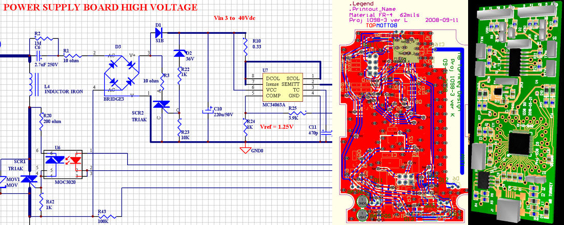
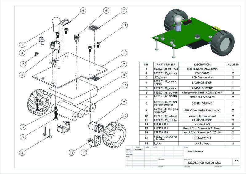
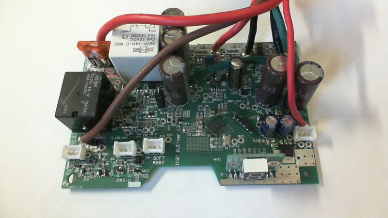
PCB Layout, PCB Layout Design, and PCB Layout Services are available for many different applications. We use Protel schematic capture and PCB layout software. Our engineers will produce a high quality, cost-effective PCB layout design from one to twelve circuit layers. We have experience with surface mount components, through-hole components, and designs that use a mixture of component mounting technologies. We also provide rapid turn-around for prototype PCBs tailored to your schedule. If you need the best of PCB layout design, PCB layout services, PCB layout, call or e-mail us.
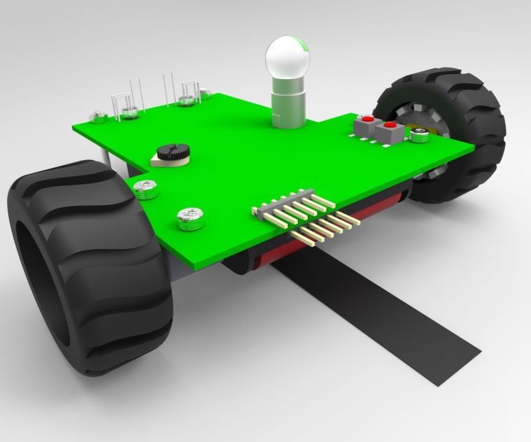
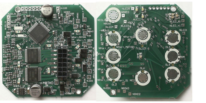
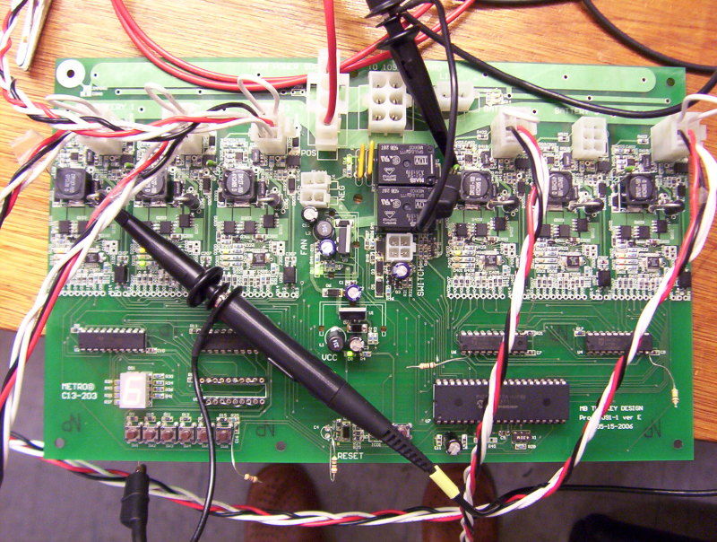
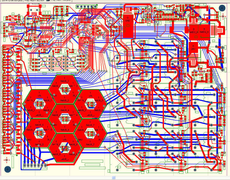
Gallery
![Final assembling drawing shows all necessary mechanical components of the device](img/pcb_n/1.jpg)
![It takes more effort and time to design small and compact board](img/pcb_n/2.jpg)
![Only experienced engineer designer will interpret correctly the correct wave shape and signal relations](img/pcb_n/3.bmp)
![The Altium and Solid Work software are compatible to exchange the data between mechanical and electronic engineers](img/pcb_n/4.jpg)
![The double side components are sometimes necessary but it will increase the cost of assembling](img/pcb_n/5.jpg)
![The PCB traces layout are made by the experienced engineer designer which is very important for the final device performance](img/pcb_n/7.jpg)
![The proper signal measurement is critical for the device reliable operation](img/pcb_n/8.bmp)
![The Protel and Altium Design Platform is the leading edge of the CAD to create a schematic PCB and simulate electrical signals](img/pcb_n/9.jpg)
![The Solid Work CAD mechanical design platform creates all metal and plastic enclosures for designed electronic devices](img/pcb_n/10.jpg)